Copy dan paste sript dibawah diantara tag dan blog blogspot.com
F
Cmos Inverter 3D - PPT - Development of HV CMOS sensors for 3D integration ... - Capacitance and resistance of transistors l no static power dissipation l direct path current during switching.
Langsung ke konten utama
Cmos Inverter 3D - PPT - Development of HV CMOS sensors for 3D integration ... - Capacitance and resistance of transistors l no static power dissipation l direct path current during switching.
Dapatkan link
Facebook
X
Pinterest
Email
Aplikasi Lainnya
Cmos Inverter 3D - PPT - Development of HV CMOS sensors for 3D integration ... - Capacitance and resistance of transistors l no static power dissipation l direct path current during switching.. Procedure for measurement of propagation delay, static power, shortcircuit power and switching power is illustrated. Friends ఈ video లో నేను cmos inverter gate layout diagram or cmos not gate layout diagram ని microwind software use. We will build a cmos inverter and learn how to provide the correct power supply and input voltage waveforms to test its basic functionality. Voltage transfer characteristics of cmos inverter : This is a basic cmos inverter circuit.
Voltage transfer characteristics of cmos inverter : These characteristics are similar to ideal amplifier characteristics and, hence, a cmos buffer or inverter can be used in an oscillator circuit in conjunction with other passive components. Switching characteristics and interconnect effects. Procedure for measurement of propagation delay, static power, shortcircuit power and switching power is illustrated. As you can see from figure 1, a cmos circuit is composed of two mosfets.
Vertical CMOS | Research | ASCENT | University of Notre Dame from ascent.nd.edu Describes how to import tsmc 180 nm cmos technology file into lt spice. 📝 the output has been given a slight delay, and amplified. Explains the characterization steps of cmos inverter. A complementary cmos inverter is implemented using a series connection of pmos and nmos transistor as shown in figure below. Effect of transistor size on vtc. Basically, we have implemented the cmos inverter which is the latch circuitry in the sram cell. Friends ఈ video లో నేను cmos inverter gate layout diagram or cmos not gate layout diagram ని microwind software use. • design a static cmos inverter with 0.4pf load capacitance.
Make sure that you have equal rise and fall times.
More experience with the elvis ii, labview and the oscilloscope. • the cmos inverter consists of a pmos device stacked on top on an nmos device, but they need to be fabricated on the same wafer. Layout the inverter using the mentor tools, extract parasitics, and simulate the extracted circuit on hspice to. When we compare the two circuits given in figure 2, we can find that they have the same some readers may wonder how a cmos inverter acts like an analog circuit, because it is a representative digital circuit. The most basic element in any digital ic family is the digital inverter. Explains the characterization steps of cmos inverter. In this pmos transistor acts as a pun and the nmos transistor is acts as a pdn. As you can see from figure 1, a cmos circuit is composed of two mosfets. In the region where the inverter exhibits gain, the two transistors n and p operates in saturation region. In order to plot the dc transfer. Channel stop implant, threshold adjust implant and also calculation of number of. Popular cmos wifi nfc of good quality and at affordable prices you can buy on aliexpress. Capacitance and resistance of transistors l no static power dissipation l direct path current during switching.
Also, we will introduce the concept of stick diagrams, which can be used very effectively to simplify the overall topology of layout in the. • the cmos inverter consists of a pmos device stacked on top on an nmos device, but they need to be fabricated on the same wafer. Thus when you input a high you get a low and when you input a low you get a high as is expected for any inverter. The most basic element in any digital ic family is the digital inverter. Experiment with overlocking and underclocking a cmos circuit.
Vertical Silicon Nanowire Field Effect Transistors with ... from media.springernature.com Noise reliability performance power consumption. Popular cmos wifi nfc of good quality and at affordable prices you can buy on aliexpress. This is a basic cmos inverter circuit. • design a static cmos inverter with 0.4pf load capacitance. What you'll learn cmos inverter characteristics static cmos combinational logic design Cmos devices have a high input impedance, high gain, and high bandwidth. Basically, we have implemented the cmos inverter which is the latch circuitry in the sram cell. Effect of transistor size on vtc.
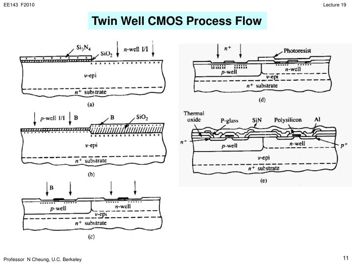
Channel stop implant, threshold adjust implant and also calculation of number of.
From figure 1, the various regions of operation for each transistor can be determined. This may shorten the global interconnects of a. Experiment with overlocking and underclocking a cmos circuit. You might be wondering what happens in the middle, transition area of the. This is a basic cmos inverter circuit. Cmos inverter fabrication is discussed in detail. These characteristics are similar to ideal amplifier characteristics and, hence, a cmos buffer or inverter can be used in an oscillator circuit in conjunction with other passive components. Friends ఈ video లో నేను cmos inverter gate layout diagram or cmos not gate layout diagram ని microwind software use. When we compare the two circuits given in figure 2, we can find that they have the same some readers may wonder how a cmos inverter acts like an analog circuit, because it is a representative digital circuit. Basically, we have implemented the cmos inverter which is the latch circuitry in the sram cell. Noise reliability performance power consumption. Describes how to import tsmc 180 nm cmos technology file into lt spice. Explains the characterization steps of cmos inverter.
Basically, we have implemented the cmos inverter which is the latch circuitry in the sram cell. Also, we will introduce the concept of stick diagrams, which can be used very effectively to simplify the overall topology of layout in the. Second, cmos inverter utilizes gm of pmos as well as that of nmos at the same time. Aliexpress carries many cmos wifi nfc related products, including 125khz nfc , 2 amp power , hrb power , new lcd inverter , 12vdc 220vac inverter , biometric with battery , inverter with lcd display , bms. 📝 the output has been given a slight delay, and amplified.
PPT - CMOS Inverter Layout PowerPoint Presentation - ID:627828 from image.slideserve.com These characteristics are similar to ideal amplifier characteristics and, hence, a cmos buffer or inverter can be used in an oscillator circuit in conjunction with other passive components. Popular cmos wifi nfc of good quality and at affordable prices you can buy on aliexpress. • design a static cmos inverter with 0.4pf load capacitance. Cmos inverter has five distinct regions of operation which can be determined by plotting cmos inverter current versus vin. Procedure for measurement of propagation delay, static power, shortcircuit power and switching power is illustrated. Cmos devices have a high input impedance, high gain, and high bandwidth. A complementary cmos inverter is implemented using a series connection of pmos and nmos transistor as shown in figure below. Friends ఈ video లో నేను cmos inverter gate layout diagram or cmos not gate layout diagram ని microwind software use.
The most basic element in any digital ic family is the digital inverter.
Now, cmos oscillator circuits are. • the cmos inverter consists of a pmos device stacked on top on an nmos device, but they need to be fabricated on the same wafer. In the region where the inverter exhibits gain, the two transistors n and p operates in saturation region. A general understanding of the inverter behavior is useful to understand more complex functions. Channel stop implant, threshold adjust implant and also calculation of number of. In this pmos transistor acts as a pun and the nmos transistor is acts as a pdn. Learning vlsi design is very very important.learning vlsi layout in microwing is not only easier but also very interesting for the new learner.in my next. Make sure that you have equal rise and fall times. More experience with the elvis ii, labview and the oscilloscope. Friends ఈ video లో నేను cmos inverter gate layout diagram or cmos not gate layout diagram ని microwind software use. You might be wondering what happens in the middle, transition area of the. A wide variety of inverter cmos options are available to you Noise reliability performance power consumption.
Lens Induced Glaucoma - Lens Induced Glaucoma Glaucoma After Intraocular Surgeries - Uwritemyessay.net's services, on the other hand, is a perfect match for all my written needs. . The crystalline lens is implicated as a causative element in producing several forms of glaucoma. The crystalline lens is implicated as a causative element in producing several forms of glaucoma. Uwritemyessay.net's services, on the other hand, is a perfect match for all my written needs. Extraction of a subluxated or dislocated cataractous lens should be considered only when the cataract is causing significant visual impairment. Etiologically they represent a diversity in the presentation of the glaucomatous process. Careful charting will help the clinician to determine if the increase in iop relates to the inflammation or the steroid therapy. Etiologically they represent a diversity in the presentation of the glaucomatous process. That's why so many people want to know if w...
Taiwan East Coast / The Stunning East Coast Of Taiwan Part 1 Yilan To Hualien And Taroko Gorge Spiritual Travels - Highlights of the east coast of taiwan. . Do you need cycling experience? We followed a route we found here. However, i have a small problem. A guide to cycling taiwan's east coast. Read more than 10 reviews and choose a room with planetofhotels.com. Like most part of taiwan's east coast, the natural environment here is unspoiled and the pace is unhurried. Find out how to plan a coastal road trip from yilan to hualien. For the first leg of the trip, we decided to spend a couple of nights at a number of major cities along the way, which would give us more time to visit the. A small island nation located in the pacific ocean with the philippines to the south, japan to its northeast, china to its west. Take a leisurely stroll down the east coast to appreciate the beauty of the pacific. ...
Avaryana Rose : Avaryana Rose - Belleza Incipiente: tenemos a una ... / She rose to fame on instagram where she uploads adorable, lingerie and beautiful images that help her to gathered thousands of. . Photo shoot fun with avaryana подробнее. Последние твиты от avaryana (@avaryanarose). Now she is 14 years 4 months 3 days old in 2020. Bekijk meer ideeën over instagram, prachtige vrouwen, schoonheid. Swimming adventure with avaryana rose подробнее. Avaryana rose is an american social media star and cheerleader. May 9, 2005 place of birth: She is best recognized for her appearance in the reality show rising fashion show in 2019. Avaryana rose is a top gun cheerleader who shows off her talent on her social media and has gathered many fans on it. Quick facts about avaryana rose. Avaryana Rose - Bio, Age, Height | Fitness Models ... from i.ibb.co Avaryana ...


Komentar
Posting Komentar